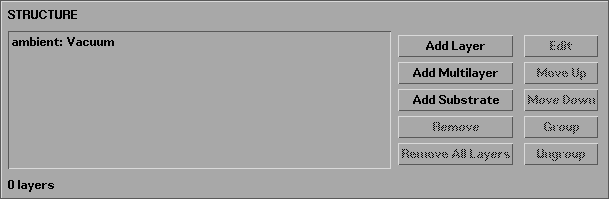
The STRUCTURE area of the main IMD widget (shown in Figure 2.1.1) consists of the Structure List, which lists the current structure elements, the buttons to the right of the Structure List, which are used to add, remove, and modify structure elements, and the Layer Count indicator below the Structure List, which indicates the total number of layers that comprise the structure.
Figure 2.2.1 The STRUCTURE area of the main IMD widget.
The techniques for defining each type of structure element - ambient, layers, and the substrate - will be described in turn below.
When IMD first starts up cold, the only structure component listed in the STRUCTURE area of the main widget is the ambient (as in Figure 2.2.1). To edit the ambient parameters, double-click on the "ambient" line in the Structure List, or select (highlight) this line and press the Edit button (to the right of the Structure List.) This brings up the Ambient widget, as shown in Figure 2.2.2.
Figure 2.2.2 IMD Ambient widget
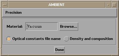
The material is the only parameter that can be specified for the ambient. (In contrast, there are many layer and substrate parameters, e.g., thicknesses, roughnesses, etc., as described below.) The default ambient material is "Vacuum". Use the techniques described in section 2.1, to change the ambient material.
In IMD, a 'multilayer structure' consists of individual layers, which can optionally be grouped together to define periodic (or aperiodic, i.e., depth-graded) multilayers. You define each layer by specifying the material comprising the layer, the layer thickness, and the interface properties: interfacial roughness, diffuseness, power-spectral-density parameters, etc.
Interface parameters are discussed in detail below.
To add a layer to the multilayer stack, press the Add Layer button to the right of the Structure List. Doing so brings up a Layer widget like the one shown in Figure 2.1.3 in the previous section. Use the techniques described in that section to specify the layer material.
For every layer, you must also specify the layer thickness, by entering the desired thickness value in thickness entry area. You can specify the desired length units (i.e., angstroms, nanometers, or microns) and precision using the Units and Precision menus.
Note: length units and precision - which affect layer thicknesses and interface parameters - are global, i.e., all layers are described by the same length units and precision, so any changes made in one layer widget will affect all others.
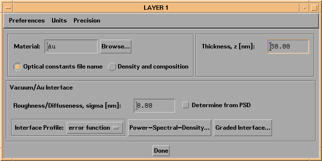
As an example, shown in the next figure is the layer widget associated with a layer of gold, 50 nm thick.
Figure 2.2.3 IMD Layer widget corresponding to a 50-nm-thick layer of gold.
To add more layers to the structure, continue to press the Add Layer button (to the right of the Structure List.) Each new layer will be inserted into the stack just below the currently selected (highlighted) layer. Use the Move Up and Move Down buttons to change the position of layers in the stack, and use the Remove and Remove All Layers buttons to delete selected layers.
The layers you create are listed in the Structure List, and are numbered consecutively (starting with layer number 1) from the top down (towards the substrate.) Layers can be edited either by double-clicking on the corresponding element listed in the Structure List, or by selecting a layer from the Structure List and then pressing the Edit button.
Any number of layers can be grouped together to create periodic multilayers. There are two ways to define such multilayers:
A. Layers that have already been added to the structure can be grouped by pressing the Group button (to the right of the Structure List), once you have selected (highlighted) the layer that you want to designate as the top of the group in the Structure List. You will then be asked to choose which layer to designate as the bottom of the group; you must choose from a list of available layers (or multilayers) that will be presented. You can then edit the periodic multilayer by double-clicking on the corresponding element in the Structure List, or by selecting the periodic multilayer in the Structure List and then pressing the Edit button.
or
B. Press the Add Multilayer button (to the right of the Structure List). You will be prompted to enter the number of different layer elements (NOT the total number of layers!) to be contained in the new periodic multilayer. Once you have entered the desired number of layer elements (and pressed the OK button), a widget appears that allows you to specify the periodic multilayer parameters.
Once layers have been grouped to form a periodic multilayer, these layers will be indented in the Structure List, and an additional line describing the multilayer parameters will be added to the list. For example, Figure 2.2.4 shows the STRUCTURE area of the main IMD widget after defining a periodic multilayer consisting of two layers. An example of the corresponding Multilayer widget is shown in Figure 2.2.5:
Figure 2.2.4 The STRUCTURE area of the main IMD widget after defining a 2-element periodic multilayer.
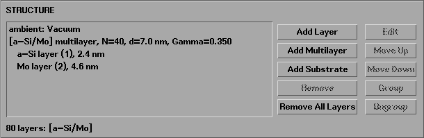
Figure 2.2.5 IMD Multilayer widget.
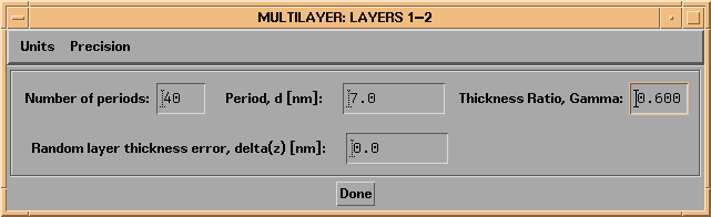
The Multilayer widget includes an area to enter parameters specific to the multilayer.
For a periodic multilayer, you must specify the Number of Periods, N, i.e., the number of repetitions of the individual layers that comprise the periodic multilayer. For example, a multilayer consisting of three different layers - A, B, and C - with N=2 periods, would contain a total of 6 layers: A/B/C/A/B/C.
The Period, d of the multilayer is determined by the thickness of the individual layers that comprise the periodic multilayer. For example, if the A, B, and C layers just described had thickness of 1, 2, and 3 nm, respectively, then the multilayer period would be d=(1 + 2 + 3)= 6 nm. (The total thickness of the periodic multilayer is N x d, or 12 nm in this example.)
The multilayer period is indicated in both the Structure List and on the Multilayer widget. The period can be specified directly only in the case of periodic multilayers consisting of just two layers, in which case the Layer Thickness Ratio, Gamma (which is defined as the thickness of the top layer divided by the multilayer period) is also indicated and available for direct specification.
If desired, you can also specify a Random layer thickness error, delta(z), in order to simulate, for example, the thickness errors that might actually occur during the growth of a multilayer film. Doing so will result in each individual layer thickness differing from the specified value by a random amount; the errors follow a Gaussian distribution with width delta(z). For example, again using the A, B, C layers with thicknesses 1, 2, and 3 nm, with N=2, choosing delta(z)=.1 nm might result in the following thicknesses: A(.997 nm)/B(2.05 nm)/C(3.01 nm)/A(1.05 nm)/B(2.01 nm)/C(3.05 nm). Note that an error will occur if you specify a random thickness error large enough to cause negative layer thicknesses.
Once you have defined a periodic multilayer, you can use the Move Up and Move Down buttons to rearrange the order of the layers (or multilayers) within the multilayer. You can remove multilayer elements (i.e., layers or multilayers) using the Remove button (once you have selected the element you wish to remove), and you can use the Add Layer and Add Multilayer buttons to insert more layers or multilayers inside of an existing multilayer.
Note: To add layers or multilayers after an existing multilayer, highlight the top line of the existing multilayer in the Structure List before pressing the Add Layer or Add Multilayer button.
You can edit layers or multilayers by double-clicking in the Structure List, or by using the Edit button after selecting the layer or multilayer you wish to edit.
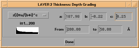
It's possible in IMD to vary with depth the layer thicknesses of any or all of the individual layers that comprise a periodic multilayer. Figure 2.2.6 shows the layer widget for a layer element that is part of a periodic multilayer containing 200 periods: note the button labelled 'Depth Grading...'. Figure 2.2.7 shows the Layer Thickness Depth Grading widget that appears when the Depth Grading... button is pressed.
Figure 2.2.6 IMD Layer widget for a layer that is part of a periodic multilayer consiting of 200 bilayers.
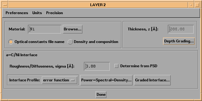
Figure 2.2.7 IMD Layer Thickness Depth Grading widget for the layer shown in Figure 2.2.6.
Four different depth grading profiles are available:
Parabolic: z(i)=a+b*i +c*i^2
Exponential: z(i)=a+b*exp(c*i)
Logarithmic: z(i)=a+b*ln(c*i)
Power-Law: z(i)=a/(b+i)^c
where i is the layer index (starting with the top-most layer in the group), z(i) is the thickness of layer i, and a, b, and c are parameters you specify. In Figure 2.2.7, a power-law depth-grading profile is shown: for the a, b, and c parameters indicated in the figure, the resultant top layer (i=1) thickness is 200 angstroms and the bottom layer (i=200) thickness is 50 angstroms. A plot of the layer thickness variation is shown in the widget as well.
Note: when you enter values for the a and b parameters, the resultant top- and bottom-layer thicknesses are computed (using the currently defined c parameter); alternatively, you can specify the top- and bottom-layer thicknesses, and the resultant a and b parameters are computed. Specifying the c parameter will result in the computation of new a and b parameters based on the current top- and bottom-layer thicknesses. (Got that?)
Each layer in a multilayer can have it's own depth grading profile (or no depth grading at all, of course). However, if you wish to grade every layer element in a multilayer by the same relative amount, you can either specify identical profiles and proportional depth grading parameters for each layer, or else make use of Coupled Parameters, as described in Section 2.3 (the latter method is much simpler.) See Section 2.5 for a graded multilayer example.
Periodic multilayers can be nested inside one another if so desired. For example, suppose you wish to create a multilayer stack consisting of five different materials (A, B, C, D, E), arranged as follows:
A/B/C/D/E/D/E/A/B/C/D/E/D/E/A/B/C/D/E/D/E.
A shorthand notation for this 21-layer structure is [A/B/C/[D/E]x2]x3
One way to create such a structure would be as follows: (a) Use the Add Multilayer button to create a periodic multilayer consisting of 2 periods of the D and E layers; (b) Use the Add Layer button three times to insert the A, B, and C layers on top of the [D/E] multilayer, and then (c) use the Group button to define the A/B/C/[D/E] multilayer, by selecting the A layer as the top element of the group, and the [D/E] multilayer as the bottom element.
In some cases, for example when you wish to model a structure consisting of a very large number of unique layers, rather than using the Add Layer button repeatedly, it is more convenient to read in a text file containing the required layer information (i.e., materials, thicknesses, etc.). To do this, use the File->Open Layer-Data File option from the menu bar. You will find instructions on how to create such a file in the sample_layerfile.txt file (or in the .xcl, .wkz, and .slk spreadsheet versions of this file) located in the directory called examples.dir in the imd directory. Also, once you have created a layer structure in IMD, you can save the layer information to a Layer-Data file using the File->Save to Layer-Data File option from the menu bar.
Note: when saving to a layer-data file, all layer-group information is lost.
Note: layer-data files can only use materials specified by reference to optical constant data files; materials specification by density and composition is not possible with layer-data files.
The final component of an IMD structure is the substrate. Use the Add Substrate and Remove buttons to add and remove a substrate. A substrate is specified in a way entirely analogous to the way a layer is specified, except that a substrate has no thickness, i.e., a substrate is a semi-infinite slab of material. If no substrate is selected, the ambient material is used on both sides of the multilayer stack.
Note: a structure consisting of just the ambient and a substrate is valid, allowing you to simulate the optical properties of a front-surface mirror.
Interface imperfections, i.e., interfacial roughness and diffuseness, have the effect of reducing the specular reflectance of an interface either by scattering light into non-specular directions, in the case of interfacial roughness, or by increasing the transmittance of the interface, in the case of interfacial diffuseness. A number of options are available in IMD to account for the effects of imperfect interfaces on the specular and non-specular optical functions. These options are described below.
Note: Each interface in the IMD structure is described by it's own set of interface parameters. Specifically, you can specify the interface parameters for the top surface of the substrate and the top surface of every layer element. In the case of periodic multilayers, note that there are two types of interfaces associated with the top layer in the stack. Thus, for example, in the case of a periodic multilayer containg A and B layers, with A on top of B, there are three different types of interfaces: A-on-B, B-on-A, and ambient-on-A. (Assuming there are no other layers on top of the A/B periodic multilayer.)
MODIFIED FRESNEL COEFFICIENTS: INTERFACE WIDTHS AND INTERFACE PROFILE FUNCTIONS
For the calculation of specular optical functions in IMD, the modified Fresnel coefficient formalism is used, as described in reference [2]. In the case of specular optical functions, the effects of interfacial roughness and interfacial diffuseness are indistinguishable: both types of imperfections reduce the reflectance of the interface. Thus, the interface can be characterized simply in terms of an interface profile function, p(z) (described below) and the interfacial width, sigma, as shown in Figure 2.2.8.
Figure 2.2.8. Imperfect interfaces: roughness and diffuseness.
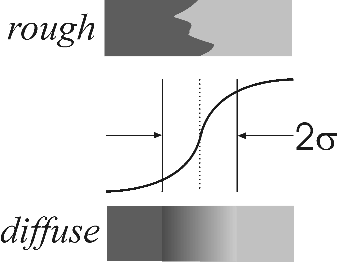
In the case of a purely rough interface, the value of sigma refers to the rms interfacial roughness, sigmar. In the case of a purely diffuse interface, sigma refers to the interfacial diffuseness, sigmad. In the general case of an interface that is both rough and diffuse, sigma = sqrt(sigmar2 + sigmad2).
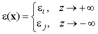
The interface profile function, p(z), is defined as the normalized, average value along the z direction of the dielectric functions, epsilon(x):
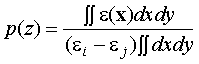
where
The resultant loss in reflectance due to interface imperfections is approximated in IMD by multilplying the Fresnel reflection and transmission coefficients by the functions w(s), the Fourier transform of w(z)=dp/dz, as described below. Five types of interface profile functions are available in IMD. These functions, and their Fourier transforms, are summarized in Table 2.2.1.
Table 2.2.1. Interface profile functions and Fresnel coefficient modification factors available in IMD.
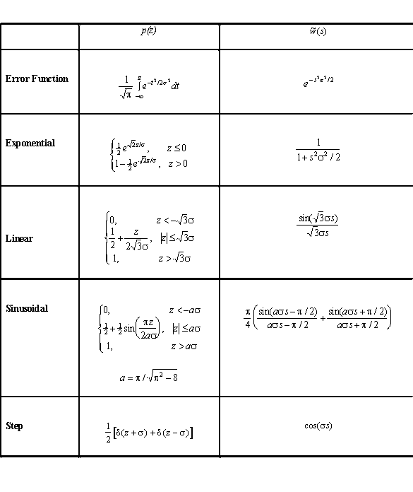
As can be seen in Figures 2.2.3 and 2.2.6 above, a droplist on the Layer widget is used to select an interface profile function. The sigma value can be entered on the Layer widget as well, or, as will be described below, when you select the Determine from PSD button, the sigma value can be computed directly from the power-spectral-density function.
You can also specify precisely how you wish to modify the Fresnel coefficents used to compute specular optical functions, specular electric field, and the electric fields used to compute non-specular optical functions. The Modified Fresnel Coefficient Preferences widget, shown in Figure 2.2.9, is available from either the File->Preferences menu option on the main IMD widget, or from the Preferences menu option availabel on all Layer and Substrate widgets. As shown in Figure 2.2.9, there are three options available:
Figure 2.2.9. Fresnel coefficient modification options.
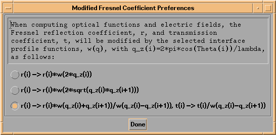
In the first option, the Fresnel reflection coefficient at the top surface of layer i is multiplied by w(2*q_z(i)), where q_z(i)=2 pi cos(Theta(i))/lambda, Theta(i) is the propagation angle in the layer (determined from the incidence angle through Snell's law,) and lambda is the wavelength of light. The function w corresponds to the interface profile function you specify, as in Table 2.2.1.
In the second option, the reflection coefficient is multiplied by w(2*sqrt(q_z(i)*q_z(i+1))), (the so-called Nevot-Croce factor,) in accord with the formalism described in reference [3] which is valid below the critical angle of total external reflection in the X-ray region.
In the third option, both the reflection and the transmission coefficients are modified, as indicated in the Figure, in accord with the formalism described in reference [4].
POWER-SPECTRAL-DENSITY FUNCTIONS
For the calculation of non-specular optical functions, it is necessary to specify the power-spectral-density (PSD) function of each interface in the structure. The PSD function can also be used to compute the sigma values used in specular optical functions computations, by selecting the Determine from PSD button on the associated Layer or Substrate widget.
Two power-spectral-density functional forms are available in IMD, as indicated in the Power-Spectral-Density Function Preferences widget shown in Figure 2.2.10. This widget is accessible either from the File->Preferences menu option, or from the Preferences menu available on all Layer and Substrate widgets.
Figure 2.2.10. The Power-Spectral-Density Function Preferences widget.
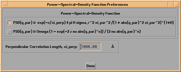
In the case of the first PSD function shown in Figure 2.2.10 (described in reference [10],) each interface is characterized by three parameters: the interfacial roughness, sigma_r, the in-plane, or parallel correlation length, xi_par, and the so-called jaggedness factor, H. In addition, a (global) vertical or perpendicular correlation length parameter, xi_perp, can be specified as well, in order to account for correlated roughness in a multilayer. Following the formalism described in reference [8], the vertical correlation function describing the correlation between two interfaces i and j is given by
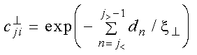
where j<=min(j,i), and zn is the thickness of layer n. The perpendicular correlation length, xi_perp, is specified on the Power-Spectral-Density Function Preferences widget.
The second PSD function available is based on the stochastic model of thin film growth and erosion described in reference [9]. In this case, the (intrinsic) PSD at each interface is characterized by the three parameters Omega, the volume element growth parameter, nu, the relaxation coefficent, and the exponent n; the intrinsic PSD also depends on the layer thickness z. (In the case of the substrate PSD, z does not necessarily refer to the substrate thickness, but is just another parameter that you must specify.) Note that in accord with this model of film growth, the total PSD at a given interface is equal to the intrinsic PSD at that interface (as specified by the Omega/nu/n/z parameters for that interface) plus the contribution of the PSD's of all the underlying interfaces; the amount of roughness that is replicated from layer to layer depends on the PSD parameters of each of the interfaces involved. Thus, this PSD model can be used to account for the evolution of roughness throughout a multilayer stack.
Note: The PSD function you select in the Power-Spectral-Density Preferences widget will apply to all interfaces in the structure you define.
Shown in Figure 2.2.11 is the Power-Spectral-Density Function widget associated with a layer that is part of a periodic multilayer, for the case of the sigma_r/xi_par/H PSD model. This type of widget appears when you press the Power-Spectral-Density... button of a Layer or Substrate widget.
Figure 2.2.11. A Power-Spectral-Density Function widget, for the case of the sigma_r/xi_par/H PSD model.
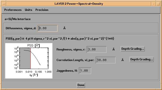
Note that a graph of the PSD function is displayed in the widget, over the range of transverse momentum values, q_par associated with the incidence and scattering angles you define, as described in Section 2.3 (The range of q_par values associated with the non-specular scattering parameters you define are indicated by the grey region in the plot.)
Note: In the case of layers that are part of periodic multilayers, as in Figure 2.2.11, it is possible to define depth-graded sigma_r and xi_par parameters as well, by pressing the Depth Grading... buttons shown in the widget. You will then be presented with a Depth Grading widget completely analagous to the graded-thickness widgets described above.
Similarly, shown in Figure 2.2.12 is the Power-Spectral-Density Function widget for the case of the Omega/nu/n PSD model.
Figure 2.2.12. A Power-Spectral-Density Function widget, for the case of the Omega/nu/n PSD model.
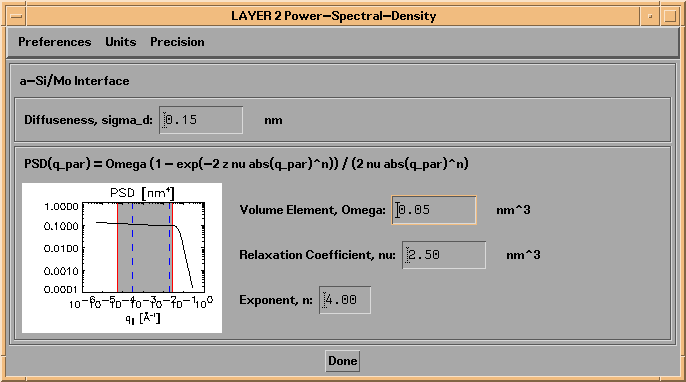
As can be seen in Figures 2.2.11 and 2.2.12, in addition to specifying the PSD parameter values for the interface, you can also specify a value of the interface diffuseness, sigma_d. The value of sigma_d will be used (along with the interface profile function you select) to compute the modified Fresnel coefficents (using the specified form of the Fresnel coefficient modification factors (Figure 2.2.9)) when computing the electric fields needed for non-specular reflected intensity calculations. (See references 4-8.)
If you have selected the Determine from PSD button on a Layer or Substrate widget, the sigma value used for that interface for computing specular optical functions via the modified Fresnel coefficient formalism described above will be equal to the value of sqrt(sigmar2 + sigmad2). In the case of the sigma_r/xi_par/H PSD model, the sigmar value used to compute tho total sigma value is just equal to the value of sigma_r that you specify on the PSD parameters widget. On the other hand, in the case of the Omega/nu/n PSD model, sigmar2 is given by:
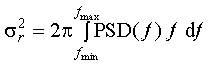
where fmin = 1 / Lmax , fmax= 1 / Lmin , and Lmin and Lmax must be specified by you, on the Power-Spectral-Density Function Preferences widget, as shown in Figure 2.2.13. The q values (where q=2 pi f,) corresponding to the values of Lmin and Lmax you enter, are indicated as dashed blue lines in the PSD plots on the Power-Spectral-Density Layer and Substrate widgets, as can be seen, for example, in Figure 2.2.12.
Figure 2.2.13. The Power-Spectral-Density Preferences widget, showing entry areas for Lmin and Lmax available when using the Omega/nu/n PSD model.
Independent of the interface profile function, sigma, and PSD parameters you specify for a given interface, in IMD it's also possible to model the effects of a diffuse interface on the specular and non-specular optical functions by specifying a 'graded' interface. That is, an abrupt interface can be replaced by one or more layers whose optical constants vary gradually between the values for the pure materials on either side of the interface.
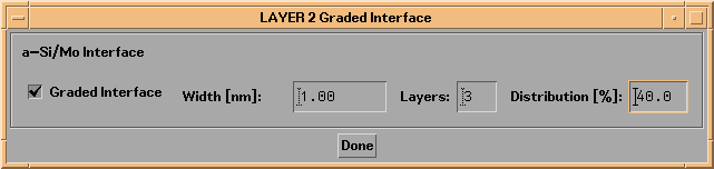
In IMD, a graded interface is described by three parameters, as shown in Figure 2.2.14: the interface width, wg, the number of layers comprising the graded interface, Ng, and the distribution factor, Xg, which determines where the graded interface region resides relative to the original abrupt interface (as will be described below.)
Figure 2.2.14. A graded interface.
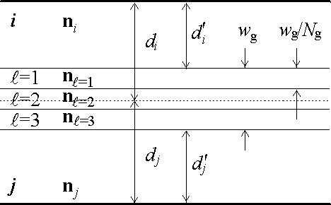
The optical constants in each of the Ng layers of a graded interface are computed as follows. Consider the graded interface between the ith and jth layers in a multilayer stack. The thickness of each of the Ng graded interface layers is equal to wg/Ng. The optical constants in the lth graded interface layer are thus given by
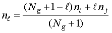
and
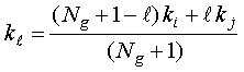
with l=1,...Ng. The resulting layer thickness, di' and dj' of the pure materials in the ith and jth layers, respecitively, after including the graded interface layers, are given by
![]()
and
![]()
with 0 < Xg < 1. (Note that the total thickness of the two layers - including all the graded interface layers - is constant, i.e., di' + dj' + wg = di + dj.) As an example, a distribution factor of 50% (Xg = 0.5) would result in equal reductions of the ith and jth layer thicknesses.
To specify a graded interface in IMD, press the Graded Interface... button on the relevant Layer or substrate widget. Doing so will cause a Graded Interface widget to appear, as shown in Figure 2.2.15, in which you can specify values for the graded interface number of layers, the interface width, and the distribution factor.
Note: you must not specify graded interface parameters that result in layer thicknesses less than zero; doing so will cause the optical functions computation to be aborted.
Note: the same interface profile function, sigma, and PSD parameters are applied to every interface in a graded interface.
Figure 2.2.15. A Graded Interface widget.